
Q Sketch
Author:Peir-Ru Wang
\(\to\)中文版
Update
(S31)2025.04.29: Gate-tunable superconducting diode effect in a three-terminal Josephson device
(S29)2025.04.28: Wafer Scale \(MgB_2\)
(S27)2025.04.27: Sketch on Quantum Error, Error Correction, and Error Protection (II)
(S25)2025.04.26: Gatemon (Ge type)
(S23)2025.04.25: Gatemon
(S21)2025.04.24: Sketch on Quantum Error, Error Correction, and Error Protection (I)
(S19)2025.04.23: Prepare for Quantum Measurement: Interaction Basis
(S17)2025.04.18: About Flux-Pumped Josephson Parametric Amplifier (JPA)
(S16)2025.04.17: About Current-Pumped Josephson Parametric Amplifier (JPA)
(S15)2025.04.16: About Quantum Signal Amplify
(S14)2025.04.14: Transmon-Spin Hybrid Qubit
(S13)2025.04.13: Andreev Bound State (2010)
(S12)2025.04.12: Hybrid Type of Fluxonium (QuTech, 2021)
- 2025.04.12: Hybrid Type of Fluxonium (QuTech, 2021)
- Spin quantum dot qubits operate at temperatures \( \leq 1K\), and their operating electrodes often enter a superconducting state.
- Andreev qubits are qubits fabricated using Andreev reflection. You can refer here.
- Topological qubits often use nanowires placed on a superconductor, utilizing the Proximity Effect to induce superconductivity in the nanowire and generate topological quantum states at the ends.
- 2025.04.13: Andreev Bound State (2010)
- 2025.04.14: Transmon-Spin Hybrid Qubit (2024)
- 2025.04.16: About Quantum Signal Amplification
- 2025.04.17: About Current-Pumped Josephson Parametric Amplifier (JPA)
- 2025.04.18: About Flux-Pumped Josephson Parametric Amplifier (JPA)
- 2025.04.23: Prepare for Quantum Measurement: Interaction Basis
- 2025.04.24: Sketch on Quantum Error, Error Correction, and Error Protection (I)
- 2025.04.25: Gatemon
- 2025.04.26: Gatemon (Ge type)
- 2025.04.27: Sketch on Quantum Error, Error Correction, and Error Protection (II)
- 2025.04.28: Wafer Scale \(MgB_2\)
- 2025.04.29: Gate-tunable superconducting diode effect in a three-terminal Josephson device
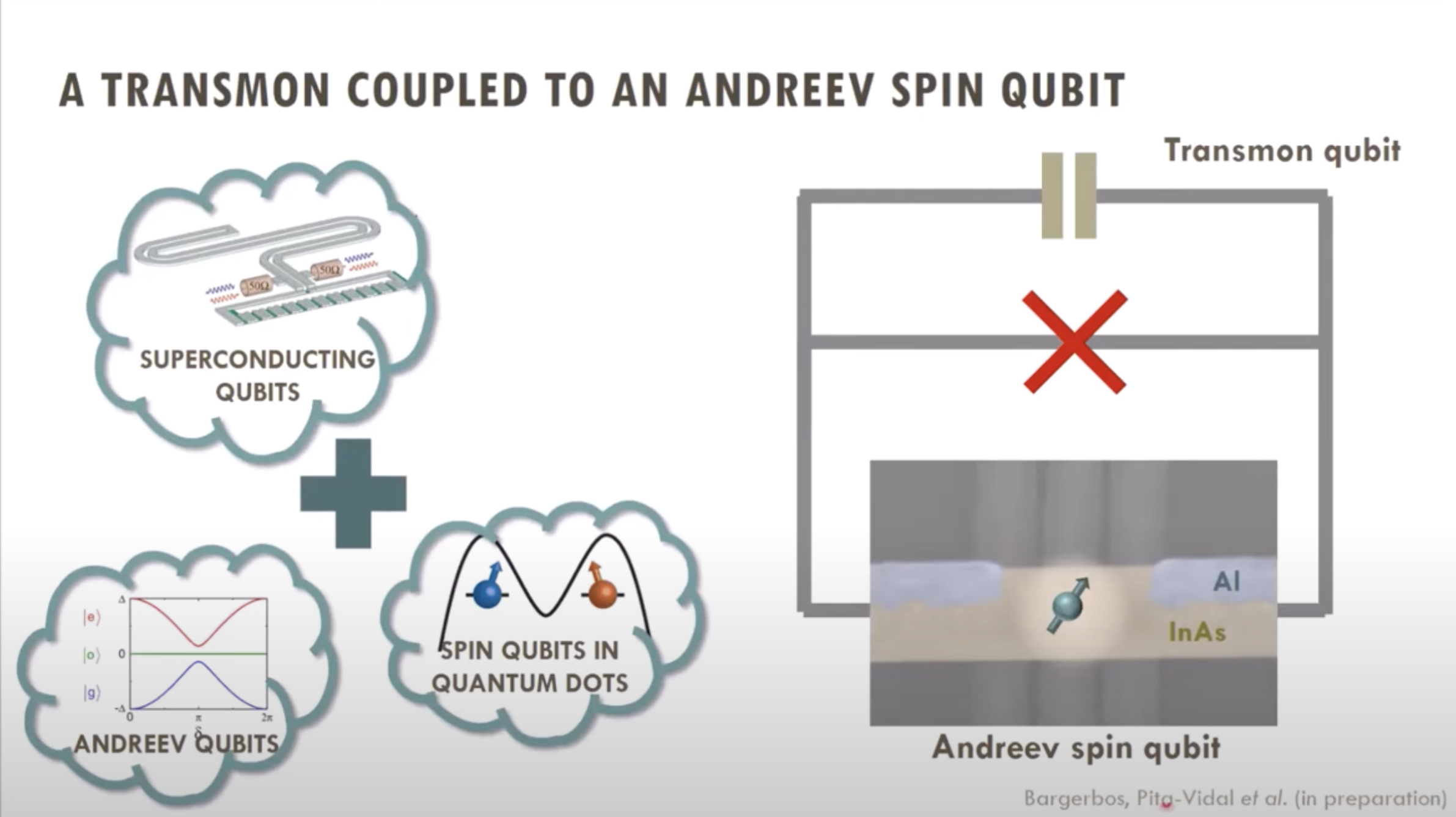
This piece references a talk from QuTech.
The talk listed five types of qubits being researched at QuTech: superconducting qubits, spin quantum dot qubits, nitrogen-vacancy diamond qubits (NV center), Andreev qubits, and topological qubits.
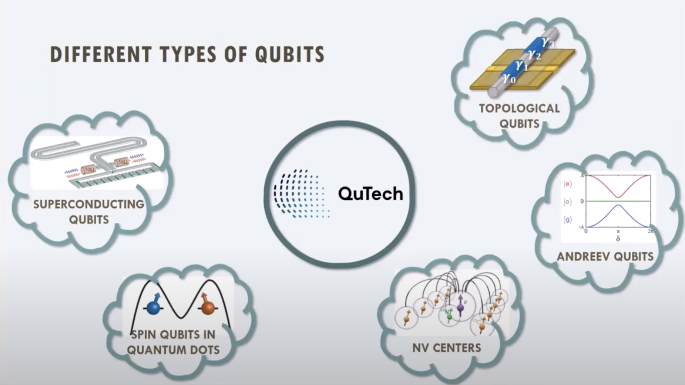
Interestingly, apart from nitrogen-vacancy qubits, spin quantum dot qubits, Andreev qubits, and topological qubits are all somewhat related to superconductivity.
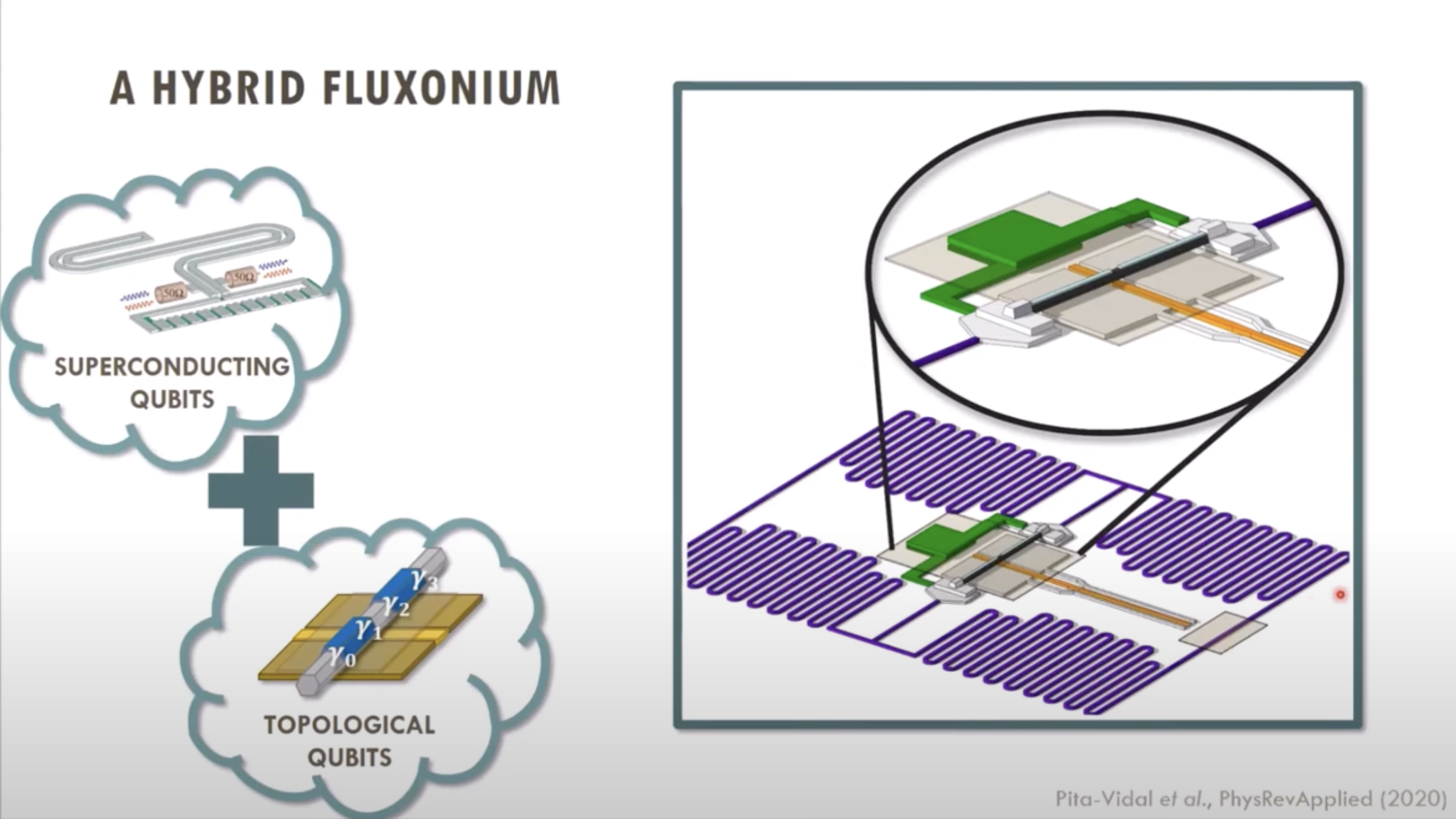
The topological qubit used here is an \(InAs)\ nanowire.
Ref:
\(\to\)Youtube: "Hybrid Devices for Quantum Computing" by Marta Pita @ QuTech, TU Delft, https://www.youtube.com/watch?v=DWfjBdQMYCI
\(\to\)Gate-Tunable Field-Compatible Fluxonium, 2020, 10.1103/PhysRevApplied.14.064038
So-called Andreev reflection occurs at a non-superconductor/superconductor interface. Since the principle of superconductivity involves Cooper pairs formed by two electrons, while the charge carriers moving in a non-superconductor are individual electrons, when a single electron tunnels from the non-superconducting material into the superconductor, it must form a Cooper pair. Charge conservation requires the reflection of a hole back into the non-superconductor. In a superconductor/non-superconductor/superconductor junction, an Andreev Bound State forms in the intermediate non-superconducting region.
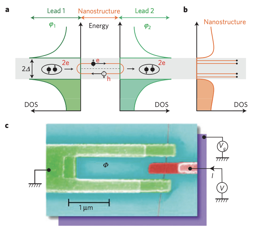
Ref: 10.1038/nphys1811
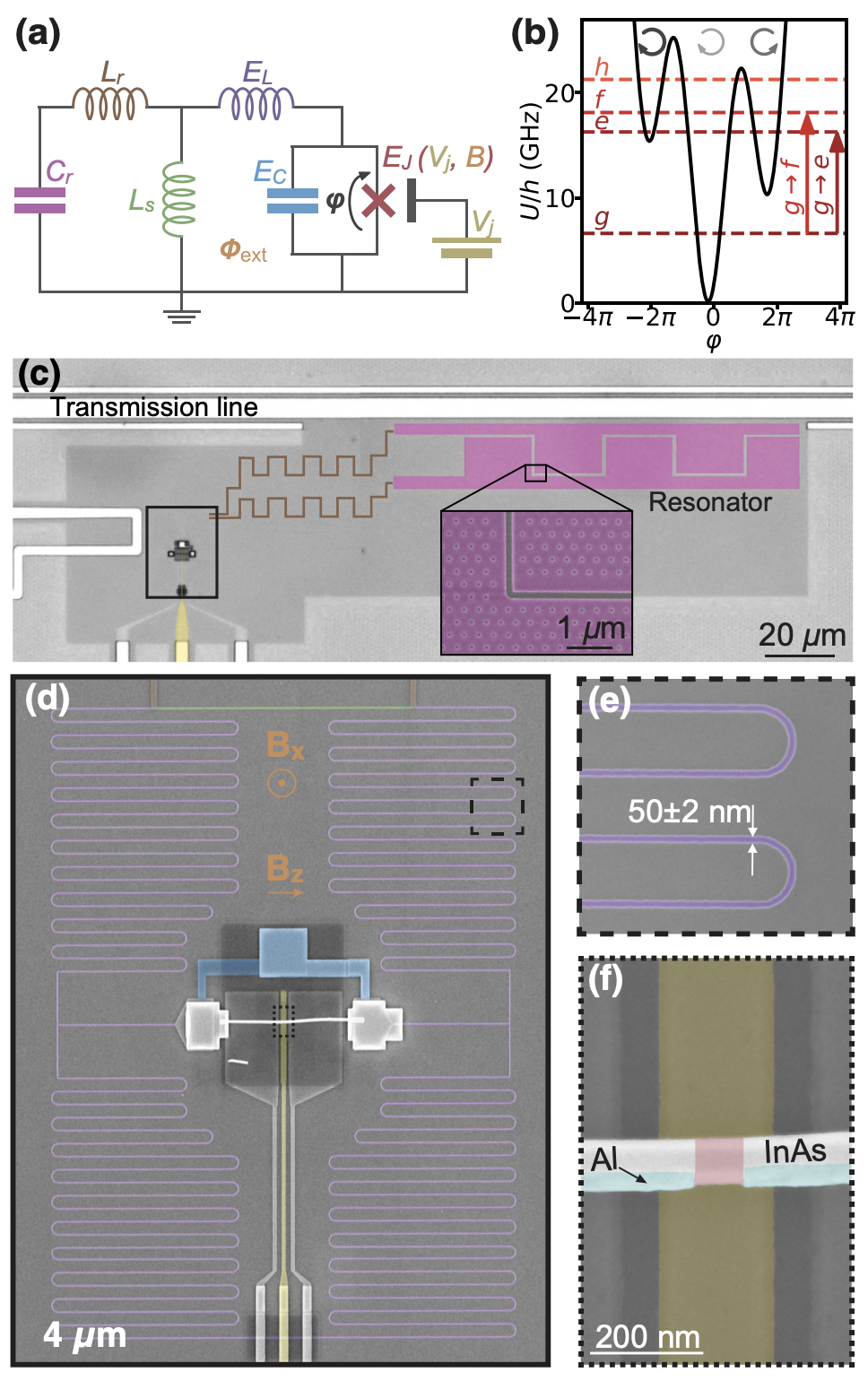
Triggered by a recent talk from QuTech\(^a\), this article explores the integration of different types of qubits. Here we introduce an interesting work combining a Transmon with a Spin Qubit.
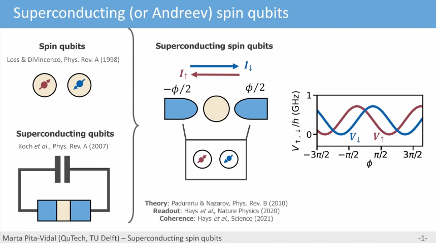
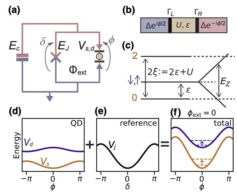
Cited from \(^b\), due to the spin-active interface, the Josephson junction properties become spin-dependent, resulting in asymmetric behavior.
Cited from \(^c\), a Josephson junction on one side of the SQUID is replaced with a spin-active interface. Through the superconducting current, it is possible to read out the state of the spin qubit. The motivation behind this type of research lies in the fact that superconducting qubits are currently the most accessible for building quantum circuits, while traditional spin qubits, although they possess longer coherence times, are harder to control. Therefore, integrating spin qubits into superconducting circuits may enable the use of mature circuit QED techniques to drive spin qubits.
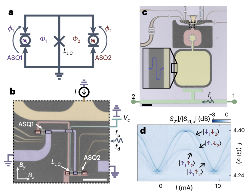
Cited from \(^d\). The previous study demonstrated a superconducting circuit coupled to a single spin qubit. However, realizing quantum computation requires multiple qubits to interact. Further experiments showed that using superconducting circuits, it is possible to generate tunable coupling between two non-adjacent spin qubits.
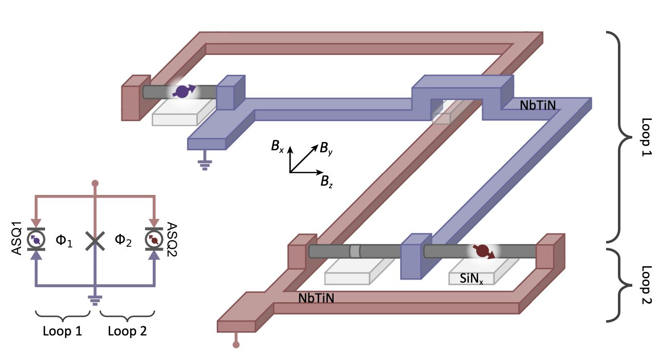
Cited from the Supplement of \(^d\). This is a schematic of the circuit used in the experiment demonstrating tunable coupling between two distant spin qubits via a superconducting circuit.
Ref:
\(^a\) Youtube: "Hybrid Devices for Quantum Computing" by Marta Pita @ QuTech, TU Delft, https://www.youtube.com/watch?v=DWfjBdQMYCI
\(^b\) "Talks - Quantum Matter for Quantum Technologies 2024 - Marta PITA-VIDAL, IBM Zurich/TU Delft", https://www.youtube.com/watch?v=VEFzm_DcQ08
\(^c\) "Singlet-Doublet Transitions of a Quantum Dot Josephson Junction Detected in a Transmon Circuit", 2022, DOI: 10.1103/PRXQuantum.3.030311
\(^d\) "Strong tunable coupling between two distant superconducting spin qubits", 2024, DOI: 10.1038/s41567-024-02497-x
This article primarily refers to "A quantum engineer’s guide to superconducting qubits (2019)" \( ^a \).
To implement quantum computation, one must measure the quantum state a qubit is in (Readout). In the classical world, measurements generally do not affect the state of the physical system being measured—in physical terms, the Hamiltonian of the measurement is much smaller than the system's Hamiltonian. However, in the quantum world, the energy scale of the measurement signal is often comparable to or even larger than the system’s own energy scale, making it crucial to understand how measurement affects quantum information.
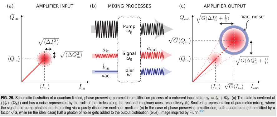
To avoid excessively disturbing the qubit, superconducting quantum circuits must reduce the energy used for readout. However, weaker signals lead to a lower signal-to-noise ratio (SNR), which often results in noise significantly interfering with the readout process. Therefore, how to "effectively" amplify weak quantum signals becomes a very important issue.
“Effectively” here means amplifying the signal in a way that is consistent with quantum mechanics and approaches the quantum limit. The concept of amplification can be simply described as: \[ s_{in} \to s_{out}=\sqrt{G} * s_{in} \] where \(\sqrt{G}\) is the amplification factor. In the quantum realm, signals are represented as frequency wave packets, and quantization of these wave packets corresponds to photons, which must satisfy the commutator relation of quantum mechanics: \[ [a_{\omega},a_{\omega}^\dagger]=1 \] where \(a_{\omega},a_{\omega}^\dagger\) represent the annihilation and creation of a photon at frequency \({\omega}\), respectively. If \(a_{\omega_{in}},a_{\omega_{in}}^\dagger\) denote the photon signal before amplification and \(a_{\omega_{out}},a_{\omega_{out}}^\dagger\) after amplification, they must still satisfy the above commutator relation. This leads to: \[ a_{\omega_{in}} \to a_{\omega_{out}}=\sqrt{G} * a_{\omega_{in}} \to \textcolor{red}{impossible !} \] which is not physically realizable. Interestingly, in the quantum world, we can achieve amplification by utilizing vacuum fluctuations from another frequency mode, called the Idler mode \(\omega_I\). Denoting this with \(b_{\omega_I},b_{\omega_I}^\dagger\), the quantum amplification process can be expressed as: \[ a_{\omega_{in}} \to a_{\omega_{out}}=\sqrt{G} * a_{\omega_{in}}+\sqrt{-1} * b_{\omega_{I}}^\dagger \]
One way to implement effective quantum signal amplification in superconducting circuits is by using a Josephson Parametric Amplifier (JPA), built with Josephson junction elements. According to energy conservation, to amplify a signal’s energy, external energy must be provided (Pump). Two common pumping methods in JPA are Current-Pumped (→ here) and Flux-Pumped (→ here).
Ref:
\( ^a \) "A quantum engineer’s guide to superconducting qubits (2019)", doi: 10.1063/1.5089550
Continuing from the previous section on quantum signal amplification, this article refers to \( ^{a,b} \) to introduce the Current-Pumped JPA.
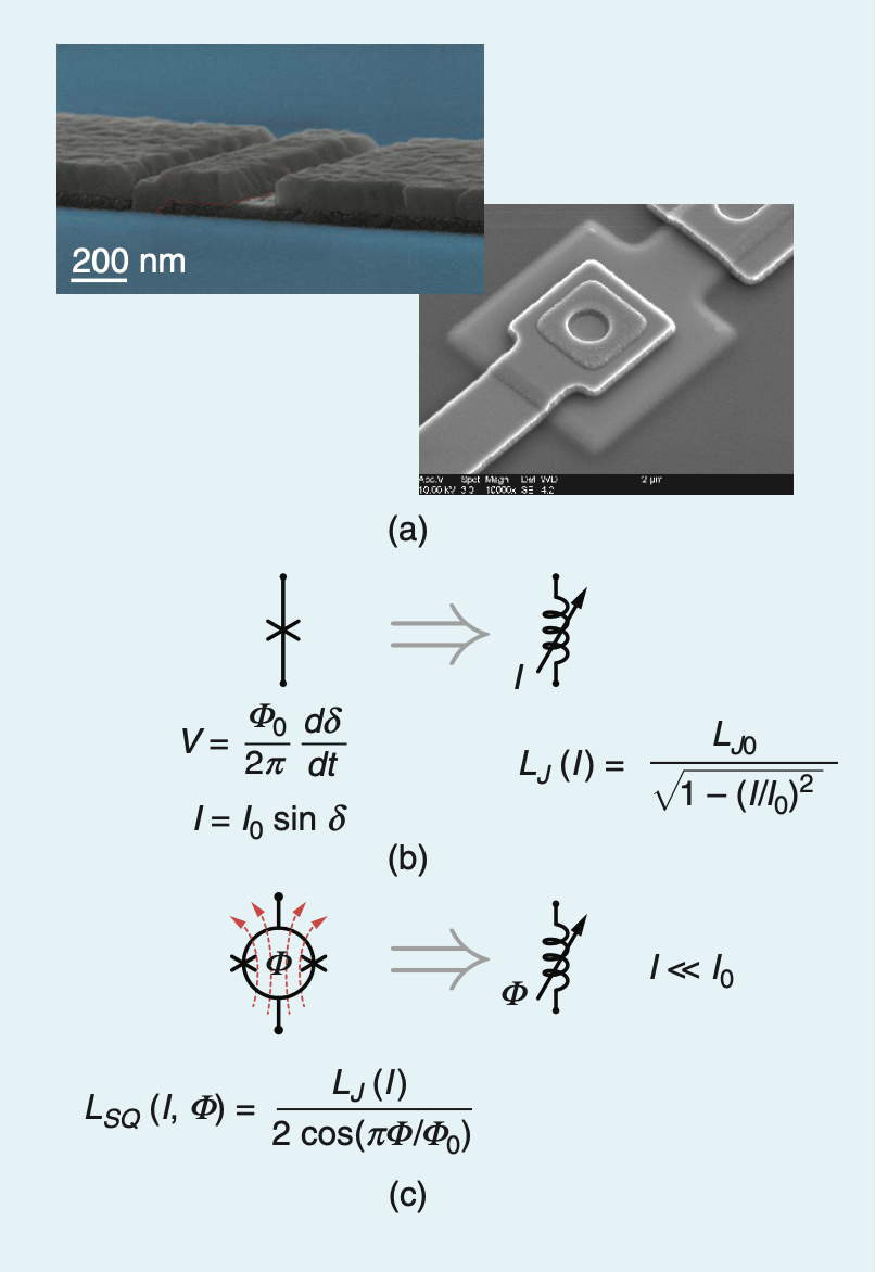
Above: (a) Josephson junction under microscope, (b) physical principle of a Current-Pumped JPA, (c) principle of a Flux-Pumped JPA. This figure is cited from \( ^a \).
Using the Josephson relation (see Superconducting Qubits): \[ \frac{I\left( \Delta \psi \right)}{I_c}=sin \Delta \psi \] \[ L\left( \Delta \psi \right)=\frac{L_0}{cos \Delta \psi}\to L\left( I \right)= \frac{L_0}{\sqrt{1-\left( \frac{I\left( \Delta \psi \right)}{I_c}\right)^2}} \] The first equation describes how applying a current \(I\) creates a phase difference \(\Delta \psi\) across the superconductors. Substituting into the second shows how the inductance \(L\) depends on the applied current. The Current-Pumped JPA uses an AC current with frequency \(\omega_p\) as the energy source.
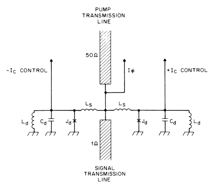
The figure above introduces the first implementation of a Current-Pumped JPA. Cited from \( ^b \).
Ref:
\( ^a \) "Superconducting Parametric Amplifiers: The State of the Art in Josephson Parametric Amplifiers (2020)", Jose Aumentad, doi: 10.1109/MMM.2020.2993476
\( ^b \) "Observation of parametric amplification and deamplification in a Josephson parametric amplifier" (1989), 10.1103/PhysRevA.39.2519
The previous section introduced the Current-Pumped JPA. This article, also referring to \( ^a \), introduces the Flux-Pumped JPA.
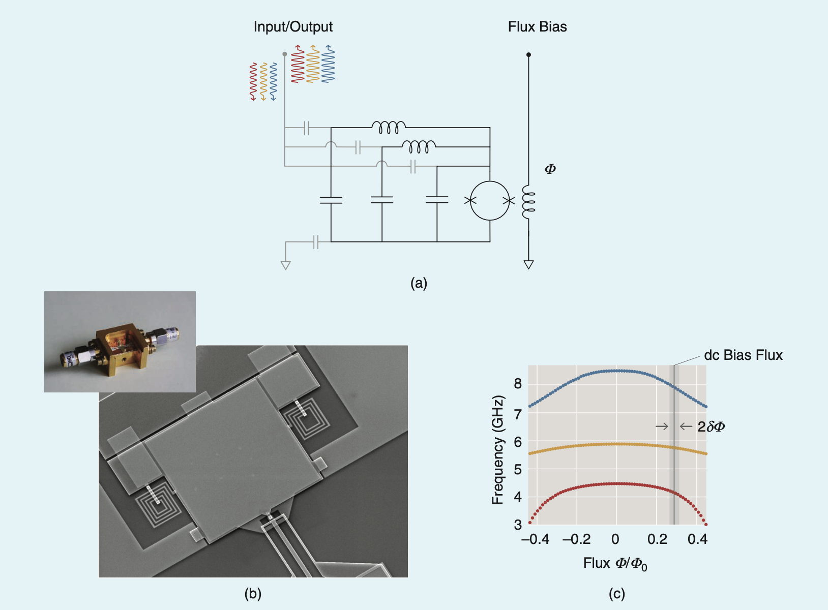
A circuit with two Josephson junctions in parallel is known as a Superconducting Quantum Interference Device (SQUID). Due to the properties of quantum electrodynamics, the quantum wavefunction couples with the electromagnetic gauge field, and the phase around the loop is affected by the magnetic flux. As previously mentioned, the inductance \(L\) depends on the phase, so a device made from a SQUID allows the inductance to be modulated via an external flux line. In this case, we can apply a time-varying magnetic flux at frequency \(\omega_p\) through the flux line to serve as the energy source.
Ref:
\( ^a \) "Superconducting Parametric Amplifiers: The State of the Art in Josephson Parametric Amplifiers (2020)", Jose Aumentad, doi: 10.1109/MMM.2020.2993476
The interaction basis is the same as the interaction picture in standard textbooks.
\[ i\hbar \partial_t |\psi_0(t)\rangle = H_0(t) |\psi_0(t)\rangle \] \[ |\psi_0(t)\rangle = e^{-\frac{i}{\hbar} \int_0^t H_0(\tau)\,d\tau} |\psi_0(0)\rangle \equiv U_0(t)|\psi_0(0)\rangle \]
\[ i \partial_t U_0(t) = H_0(t) U_0(t) \] \[ -i \partial_t U_0^\dagger(t) = U_0^\dagger(t) H_0(t) \]
\[ i\hbar \partial_t |\psi(t)\rangle = [H_0(t) + H_I(t)] |\psi(t)\rangle \] \[ |\Theta(t)\rangle \equiv U_0^\dagger(t) |\psi(t)\rangle \]
\[ \begin{aligned} i\hbar \partial_t |\Theta(t)\rangle &= i \partial_t [U_0^\dagger(t) |\psi(t)\rangle] \\ &= i\hbar \partial_t U_0^\dagger(t) * |\psi(t)\rangle + U_0^\dagger(t) * i\hbar \partial_t |\psi(t)\rangle \\ &= -U_0^\dagger(t) H_0(t) * |\psi(t)\rangle + U_0^\dagger(t)[H_0(t) + H_I(t)] |\psi(t)\rangle \\ &= U_0^\dagger(t) H_I(t) |\psi(t)\rangle = U_0^\dagger(t) H_I(t) U_0(t) U_0^\dagger(t) |\psi(t)\rangle \\ &= U_0^\dagger(t) H_I(t) U_0(t) |\Theta(t)\rangle \end{aligned} \]
\[ i\hbar \partial_t |\Theta(t)\rangle = U_0^\dagger(t) H_I(t) U_0(t) |\Theta(t)\rangle \]
A major bottleneck currently facing quantum computing is the high error rate. In gate-based quantum computers, errors can be broadly classified into single qubit errors and gate errors. This article will first focus on single qubit errors as the foundation for discussion.
Single qubit errors can be understood from the energy perspective. The evolution of a quantum state obeys the Schrödinger equation: \[ i\hbar \partial_t \ket{\psi\left(t\right)}=\hat{H}\left(t\right) \ket{\psi\left(t\right)} \leftrightarrow \ket{\psi\left(t\right)}=e^{-\frac{i}{\hbar}\mathcal{T}\left[\int^t_0\hat{H}\left(\mathscr{t}\right)d\mathscr{t}\right]}\ket{\psi\left(0\right)} \] Here, \( \mathcal{T}\left[\int^t_0\hat{H}\left(\mathscr{t}\right)d\mathscr{t} \right]\) denotes a time-ordered integral, because Hamiltonians at different times may not commute: \[ \left[\hat{H}\left(t_1\right),\hat{H}\left(t_2\right)\right]\neq 0 \] This non-commutativity makes the evolution of quantum systems more complex. If the Hamiltonians commute, the time-ordered integral simplifies to the standard form: \[ \mathcal{T}\left[\int^t_0\hat{H}\left(\mathscr{t}\right)d\mathscr{t}\right]_{\left[\hat{H}\left(t_1\right),\hat{H}\left(t_2\right)\right]= 0} =\hat{H} * t \leftrightarrow \ket{\psi\left(t\right)}=e^{-\frac{it}{\hbar}\hat{H}}\ket{\psi\left(0\right)} \]
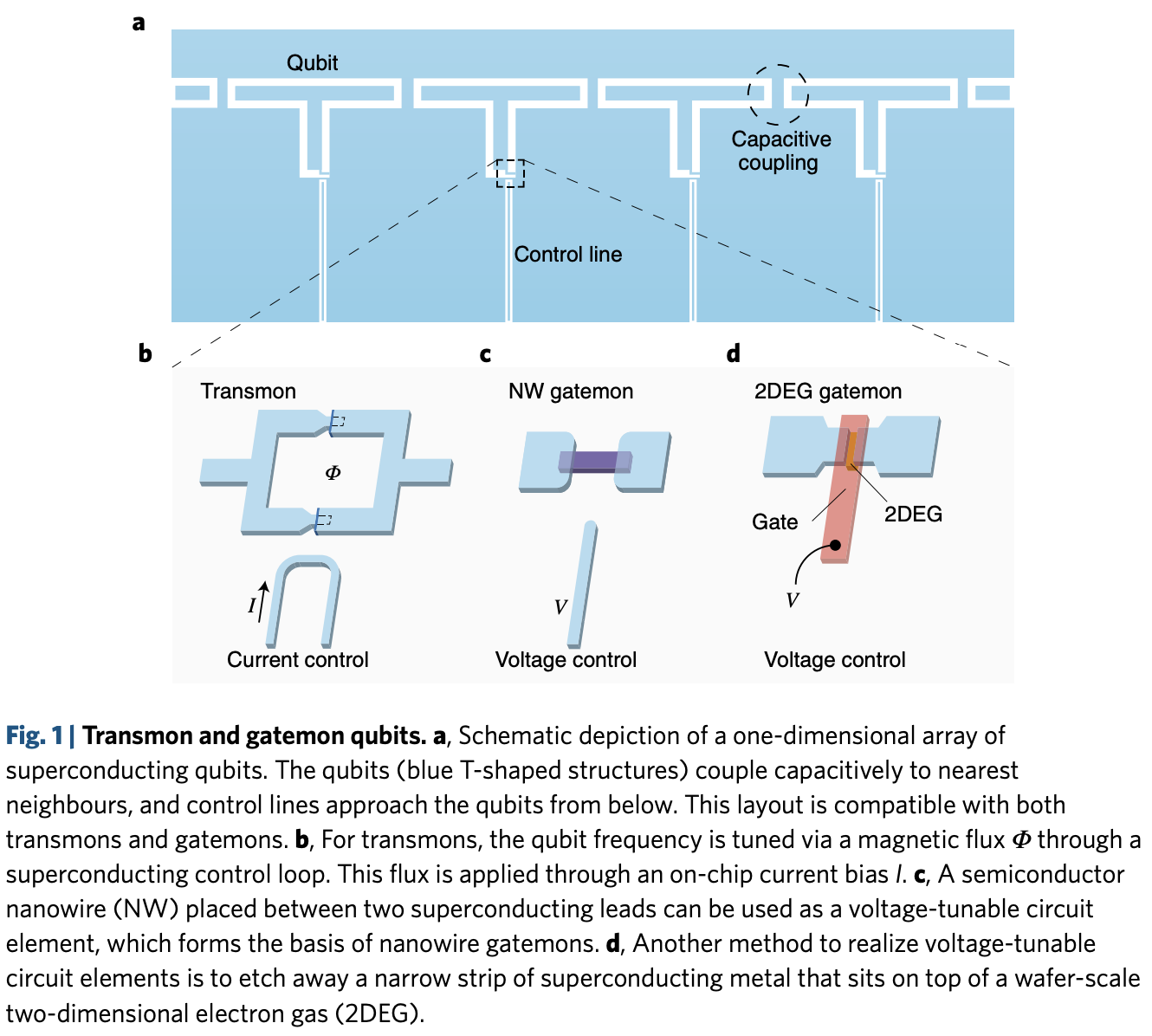
Ref. Gatemons get serious, Nature Nanotechnology (2018), Doi:10.1038/s41565-018-0218-8
Gatemon is a type of qubit based on superconducting materials, combined with a gate-defined spin qubit-like structure. A gate voltage is applied to the Josephson junction to control the qubit's properties. In the figure above (b.), within the tunable transmon, magnetic flux is applied through a flux line to adjust the effective inductance of the SQUID, thereby tuning the transmon frequency. (c, d) show two different implementations of the Gatemon.

Ref. Superconducting gatemon qubit based on a proximitized two-dimensional electron gas, Nature Nanotechnology (2018), Doi:10.1038/s41565-018-0207-y
The figure above shows an Al-based Josephson junction used to control a 2DEG (two-dimensional electron gas) formed in InAs.
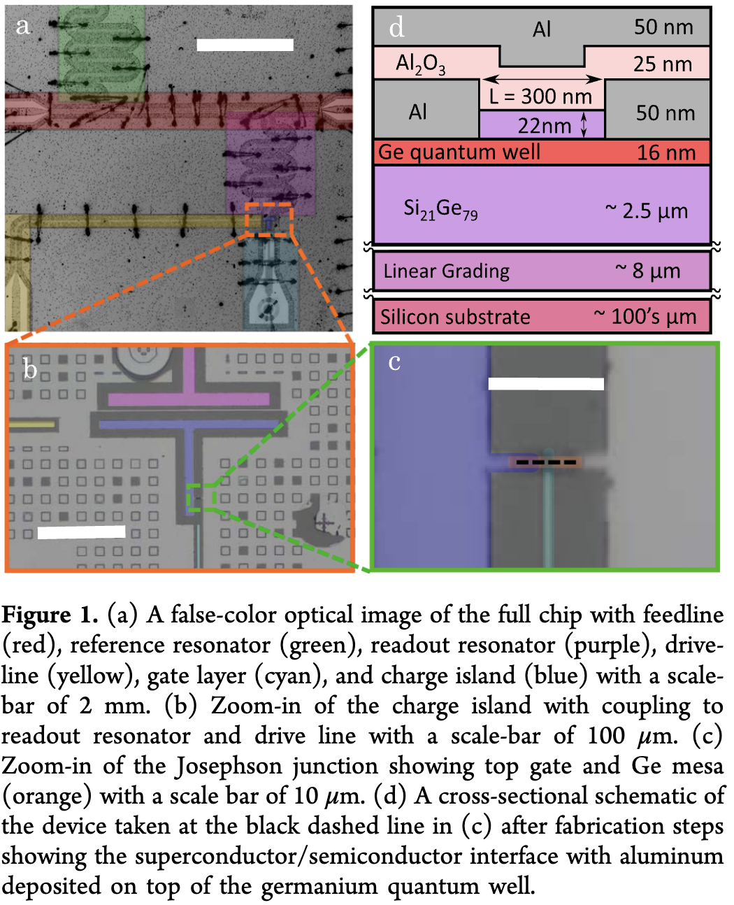
Ref. Gatemon Qubit on a Germanium Quantum-Well Heterostructure, Nano Letter (2024), Doi:10.1021/acs.nanolett.4c05539
The above figure shows an Al-based Josephson junction controlling a 2DEG in SiGe (silicon-germanium). SiGe is commonly used in gate-defined spin qubits, as referenced here. Thus, Gatemon can be viewed as a hybrid of superconducting circuits and gate-controlled qubit design, exploring novel qubit architectures.
The Hamiltonian includes the qubit's internal energy \(\hat{H}_Q\), the external control potential \(\hat{H}^I\), and noise \(\hat{H}_N\): \[ \hat{H}\left(t\right)=\hat{H}_Q+\hat{H}^I\left(t\right)+\hat{H}_N\left(t\right) \] In quantum computing, it is common to choose a "rotating frame", which is essentially the interaction basis. This involves selecting a new coordinate system that isolates the interaction and noise terms: \[ U_Q\left(t\right) = e^{-\frac{i}{\hbar} \mathcal{T}\left[\int_0^t H_Q(\mathscr{t})\,d\mathscr{t} \right]} \] \[ \ket{\Theta(t)}=U_Q^\dagger \left(t\right) \ket{\psi(t)} \] \begin{align} i\hbar \partial_t \ket{\Theta(t)}&= U_Q^\dagger(t) \left(\hat{H}^I(t) +\hat{H}_N(t) \right) U_Q(t) \ket{\Theta(t)}\\ &\equiv \left(\check{H}^I(t) +\check{H}_N(t) \right) \ket{\Theta(t)} \end{align} Here, \( \check{H}^I(t) \equiv U_Q^\dagger(t) \hat{H}^I(t) U_Q(t) \) indicates we are using the rotating frame (interaction basis), with the notation \(\, \hat{} \to \textcolor{red}{\check{}} \).
Ref. A quantum engineer's guide to superconducting qubits, Appl. Phys. Rev. 6, 021318 (2019), Doi:10.1063/1.5089550
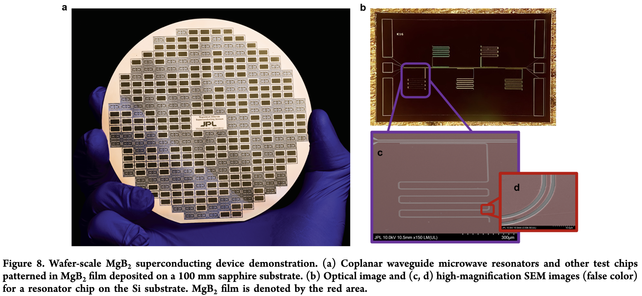
As the highest-\(T_c = 40K\) conventional superconductor (explained by BCS theory), \(MgB_2\) is a strong candidate for higher-temperature quantum bit applications. Current common superconducting qubit materials include \(Al, T_c^{Al}=1.2K\) and \(Nb, T_c^{Nb}=9.2K\), which are typically operated at \(10mK\), requiring substantial cooling power. The term "hot qubit" often refers to a qubit that can operate stably at \(1K\), which already significantly reduces the cooling demand. In thin film fabrication, having multiple elements introduces challenges in maintaining correct stoichiometry. Hence, achieving wafer-scale \(MgB_2\) is an important technical milestone.
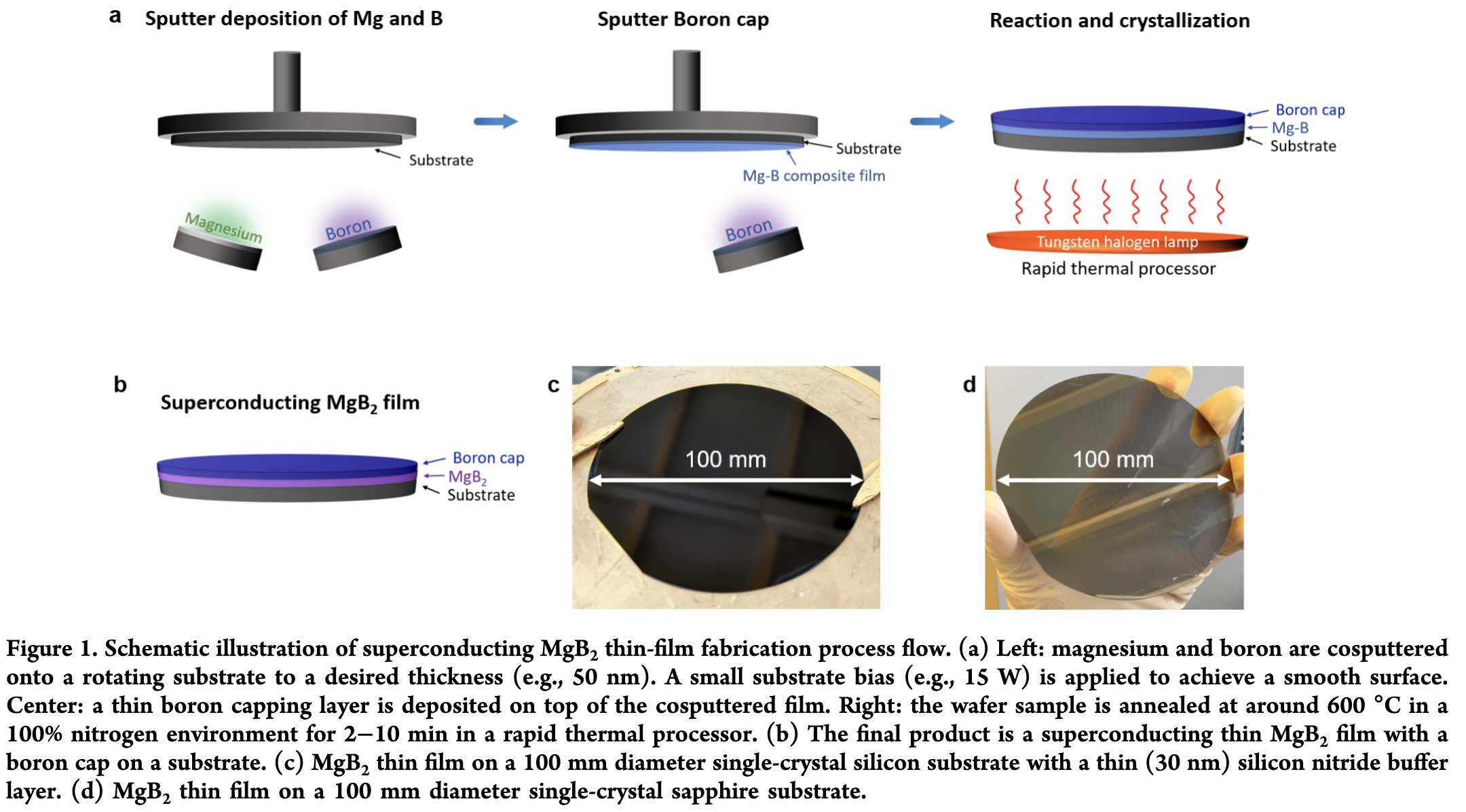
Ref. Wafer-Scale MgB2 Superconducting Devices, ACS Nano (2024), Doi:10.1021/acsnano.4c11001
Ref. Wafer-Scale MgB2 Superconducting Devices, ACS Nano (2024), Doi:10.1021/acsnano.4c11001
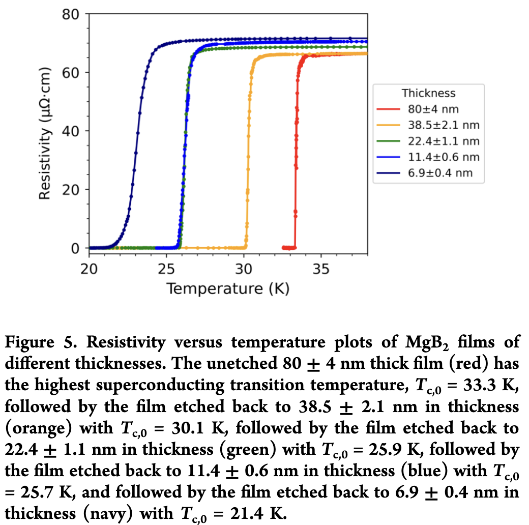
Tuning the critical temperature of superconductors has long fascinated me. During my PhD, I explored theoretical frameworks to understand how \(T_c\) could be modified, which you can read about here. The critical temperature of \(MgB_2\) can also be tuned by adjusting the film thickness.
Ref. Wafer-Scale MgB2 Superconducting Devices, ACS Nano (2024), Doi:10.1021/acsnano.4c11001
Non-reciprocal critical current in a Josephson device.
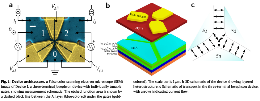
Ref. Gate-tunable superconducting diode effect in a three-terminal Josephson device, Nature Communications (2023), Doi: 10.1038/s41467-023-38856-0
後記
Index
Contact:
![]()